Analog chip layout is still drawn by hand, and the field’s consensus explanation—the netlist doesn’t carry the designer’s intent—is only half right. Some intent isn’t missing; it’s unsettled: a wager on operating conditions nobody has specified yet, so no amount of capture can recover it. That’s why the tools that matter aren’t the ones that guess your intent best on the first try, but the ones that make the tenth try cost what the first one did—tools for being wrong efficiently. Prediction: within five years the routine use of AI layout tools will be “regenerate it,” not “generate it,” and the metric that matters will be turnaround time on a changed constraint.

How automated should analog chip design be by now? In 2018 a coworker gave me his answer with a smirk: “We were told analog layout was going to be automated more than thirty years ago. It still hasn’t happened!” I was ten years into drawing analog layout at that point—it’s nearly twenty now—and I’ve been carrying his question around ever since. Digital design automated itself decades ago: synthesis and place-and-route handle billions of transistors, and nobody draws digital polygons by hand anymore. Analog layout is still drawn by hand, by specialists, at every serious semiconductor company.1 The interesting question is why.
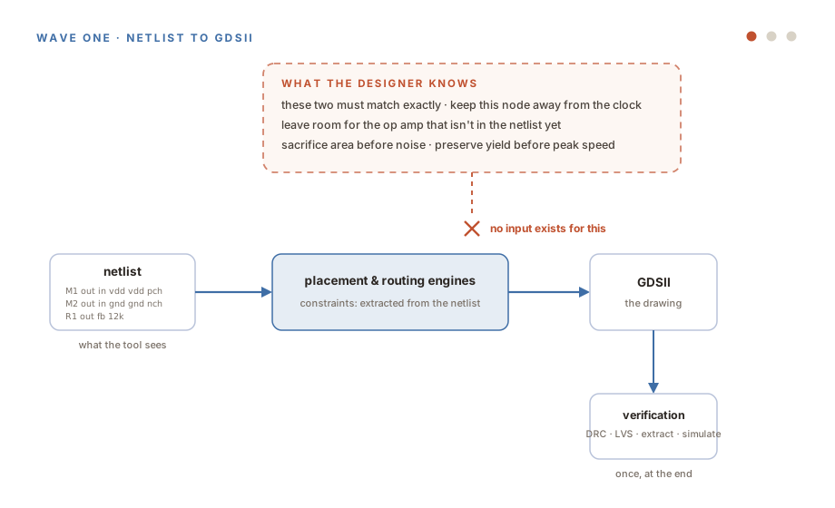
The people who build design automation have mostly converged on an answer: designer intent. A netlist tells a tool which devices exist and what connects to what, but not why—not which devices must match, which nodes are sensitive, or whether this block’s priority is noise, power, area, or yield. Tools that read only netlists were always going to plateau, so the last decade of research has gone into getting the intent in: automatic constraint extraction, learned symmetry recognition, and now language models you can simply tell what you’re protecting.
My guess is that most researchers in the field would call this the whole story. I think it’s half the story. The half about netlists is correct, and nearly everything interesting in the last decade follows from it. But there’s a quiet assumption underneath—that the intent is sitting there, complete, waiting to be captured—and anyone who’s spent a couple of decades drawing analog layout knows that assumption is wrong. A lot of the intent in my own blocks did not exist at the time I drew them. That sounds mystical, so I’ll spend most of this post defending it, because it changes what kind of tool you should actually want.
The layout is part of the circuit
First, why analog is hard to automate at all. It is not that digital design has no difficult physics—modern digital flows manage timing, congestion, IR drop, electromigration, and a dozen other effects. The difference is that digital design benefits from strong, standardized abstractions. A standard cell has a defined logical function, legal placement sites, and characterized timing; the behavior at every boundary is represented in a form automation can use. Analog interfaces carry impedance, loading, bias, noise, stability, and matching requirements that resist complete abstraction.2 Digital design is building with Lego blocks; analog design is sculpting clay.

Concretely: an amplifier’s ideal gain may depend on nothing more than a resistor ratio. But the physical implementation of those resistors also determines thermal noise, bias-current error, loading, parasitic capacitance, pole locations, and how well the ratio holds across process variation and thermal gradients. You can change the resistor geometry, preserve the nominal ratio exactly, and still shift several second-order effects at once.3 Press the clay in one place and the surrounding shape moves. In analog, the layout is not a drawing of the circuit. It is part of the circuit.
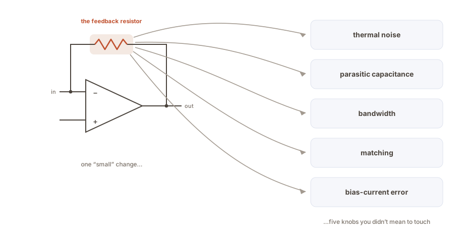
This is also why a compact layout is not automatically a good layout. A designer will deliberately leave space beside a sensitive node, split a device into matched segments, add dummies, or surround a block with a guard ring. These choices consume area, but area is one value among many—they buy matching, noise isolation, and yield. The veteran’s layout looks wasteful right up until you understand what the empty space is doing.
Sometimes the clay wins outright. I once watched a team spend the better part of a month trying to realize a clever high-speed circuit—cross-coupled connections and capacitors meant to extend an amplifier’s bandwidth. It worked in the schematic. It kept working with device parasitics added. But the cross-coupling needed nets that were short, low-resistance, and low-capacitance all at once, while physically climbing through vias from transistors on the bottom metals to capacitors near the top. Several engineers, five or six schematic revisions, small layout experiments built just to probe whether any geometry could deliver the numbers. None could. We dropped the circuit and solved the problem with a different architecture. Nothing was wrong with the circuit idea; the drawing just refused to become it. Note the shape of that failure: it isn’t that any single drawing took too long. It’s that nobody knew, going in, whether the search would finish in a week, a quarter, or at all. Hold on to that shape—it comes back at the end.
Forty years of partial credit
My coworker’s smirk implies that nobody seriously tried. In fact people have been attacking this since the 1980s, and calling their results “failures” misses what each generation contributed. IDAC (1987) sized analog circuits from a library of circuit classes; its companion ILAC (1989) generated layout from a circuit description, and its authors were honest about the gap: layouts averaging 25 percent larger than manual. KOAN/ANAGRAM II (1991) treated analog placement and routing as simulated-annealing optimization—symmetry-aware, not a naive digital placer—and its results were only as good as the constraints and cost terms it was given. Cadence’s parameterized cells in the 1990s guaranteed DRC-correct devices; Neolinear and Barcelona Design sold analog synthesis in the 2000s; Berkeley’s BAG (2013) encoded expert procedure as parameterized generators, which work well precisely within the circuit families their authors anticipated. Every era got better at feeding the tools intent. Every era hit the same wall anyway.
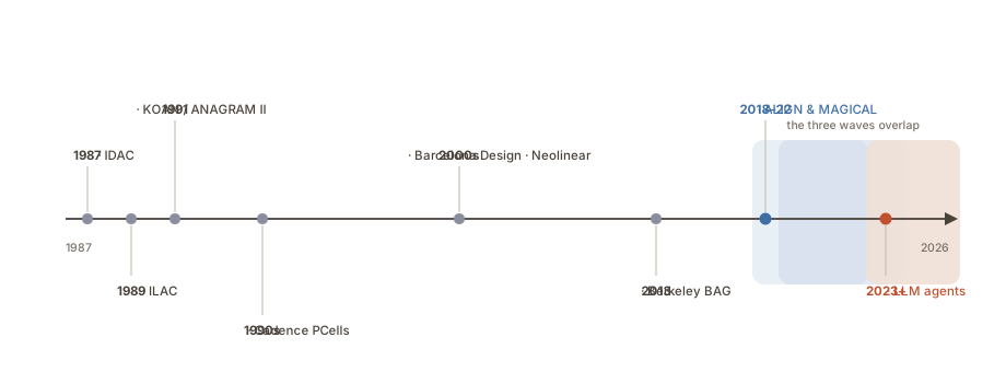
The modern era started when DARPA’s IDEA program—part of its Electronics Resurgence Initiative—funded two open-source frameworks, ALIGN and MAGICAL, that aimed to go from SPICE netlist to manufacturable geometry. MAGICAL produced the result that still anchors the field: a fully synthesized 40 nm, 1 GS/s continuous-time delta-sigma ADC, fabricated, with measured performance comparable to the manual design. Reported layout synthesis time: about 90 seconds. Not a benchmark, not a simulation—measured silicon, the top rung of the evidence ladder.4
The paper gives no baseline for what the manual layout cost, so let me supply the practitioner’s estimate: a block like that is weeks of a team’s life. Hold on to the ninety seconds, though. I think it matters more than the headline result, and I’ll come back to it.
Then wave one hit the familiar wall, just further along. At FinFET nodes the extractable constraints—the ones you can compute from the netlist—stop being enough. It’s worth being precise about what a netlist contains: which devices exist, their nominal dimensions, what connects to what, which subcircuits repeat. A process design kit adds which geometries are legal. Neither says why anything matters. The netlist shows two identical transistors; it doesn’t say whether they need exact matching, a deliberate ratio, or no matching at all. It shows a bias line; it doesn’t say whether that line’s main risk is voltage drop, noise pickup, or mismatch across a thermal gradient.
Here’s what that looks like from inside the job. A bias-current generator is a current mirror handing out copies of a reference current. The netlist shows an array of identical transistors and says they connect. It does not say they must match—so into a common array they go, dummy devices around the edge. It does not say the array has enough parasitic resistance inside it to form a small resistor ladder, which means where you tap the reference line decides how accurate the mirrored currents are. And it certainly does not say that the roadmap has another op amp coming in a future revision, needing another current—which is why I leave open space beside the array. The netlist cannot carry intent about a device that is not in it yet.
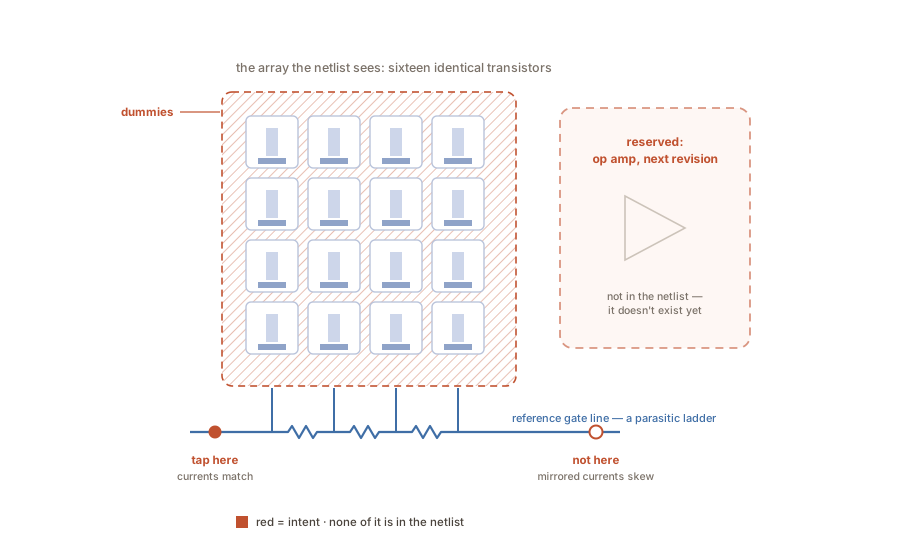
The netlist says “connect A to B.” It never says what the designer was protecting. Call this the missing-intent problem. It’s real, it’s the consensus diagnosis, and the field has spent a decade chipping away at it. If that were the whole problem, I’d expect the smirk to expire soon. It isn’t the whole problem.
The intent that doesn’t exist yet
There’s a second wall behind the first, and it’s quieter. Suppose your tool has a candidate layout and a reasonable set of constraints. How does it know whether the candidate is any good? An honest evaluation means legal geometry, DRC, LVS, parasitic extraction, then simulating the extracted circuit across process, voltage, temperature, and mismatch—anywhere from minutes to days per candidate, and an optimizer wants thousands. Machine learning offered a way through: learn a cheap approximation of the expensive evaluation. NVIDIA’s ParaGraph (2020) predicted layout parasitics from the schematic graph before any layout existed, and reported cutting average pre-layout simulation error from over 100% to under 10% on its industrial circuits. Estimate many candidates cheaply; fully verify the finalists. This changed the economics of the search, and it was still not enough—because a surrogate predicts physical consequences, and it cannot know whether a consequence matters. A few femtofarads of coupling is irrelevant between two low-impedance nodes and fatal between a clock and a high-impedance input.
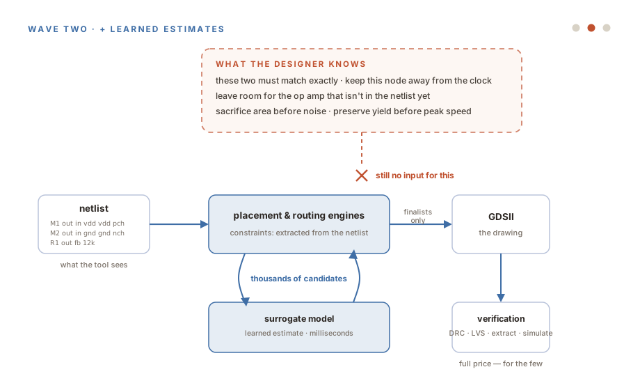
At this point the obvious response is: fine, that’s just the missing-intent problem again. Capture the designer’s intent, feed it to the optimizer, done. Here is the story that convinced me it is not that simple.
About six years into my career, after coming up as a layout designer and finishing a master’s, I asked for a circuit-design assignment of my own: a phase-frequency detector for a PLL. My first circuit designed from scratch—and, as it turned out, my only one. I built it as two half-cells and did everything I could to transmit my intent, because the layout would be done while I was on vacation: drew the schematic so the symmetry was obvious, wrote notes on it. When I came back, the half-cells weren’t mirrored. They were copied and stepped, with the power routed heavier on one side. It was not what I had asked for, and I set out to prove it mattered.
I couldn’t. I ran corners. I ran Monte Carlo for mismatch. I hunted for a dead zone for over a week—long enough that my boss’s boss made me put together a block review because I was taking too long. The layout that violated my written, explicit intent had margin everywhere I looked. I shipped it, and the product worked and was reused for years. Then the coda: generations later, another designer pushed that circuit to several times the frequency, and the asymmetry I had worried about finally started to show. Under the tighter spec we made it symmetric—by then I was managing the layout, watching my old intent become load-bearing at last. Same choice, same geometry. At one frequency it was a stylistic preference; at another it was a requirement. Nothing in the netlist—and, humblingly, nothing in my own annotations—could have told a tool which one it was that day, because the answer depended on a specification that wouldn’t exist for years.
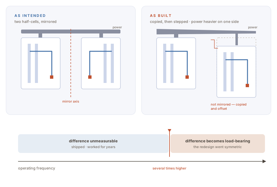
That is not a missing-intent problem. That is intent that hadn’t happened yet. So I’d split the concept in two. Some layout intent is missing: recoverable in principle, absent from the netlist in practice. Forty years of tooling has steadily chipped away at that kind, and a language interface may finish the job. And some layout intent is unsettled: a wager on operating conditions nobody has specified yet. It has no correct value at the time you draw, so no extraction, annotation, or chat interface can recover it—there is nothing to recover. The first kind is an engineering problem. The second kind sets the ceiling, and the field’s consensus answer quietly assumes all intent is the first kind.
Tools for being wrong efficiently
Which brings us to the LLM wave, and the part that changed my mind about where this is going. Language models are terrible at exact geometry—ask one to compute coordinates for a hundred interlocking polygons and it will hallucinate cheerfully. Exact geometry belongs in deterministic generators, placers, routers, and verification. What an LLM can do, and what nothing before it could, is take “match this differential pair, keep the routes electrically symmetric, isolate the input from the clock, and prioritize noise over area” and translate it into constraints, tool commands, search plans, and explanations of failed simulations. The LLM is not the sculptor. It is the first tool that speaks the sculptor’s language.
The academic results are early but real. LayoutCopilot (2025) turns plain-English instructions into commands for an interactive analog-layout tool, splitting the work across specialized agents; in one 40 nm op-amp case, interactive adjustments reduced placement area to 66% of its initial value while post-layout simulation showed common-mode rejection improving from 27.3 to 58.7 dB.5 GLayout attacked the training-data problem—real layouts are locked behind foundry NDAs—by converting layouts into a technology-generic text representation and training on fewer than 50 unique circuits. And closed-loop agents like EEsizer propose device dimensions, run the simulator, read the results, and try again.6
Now, a fair objection: maybe the language model isn’t the decisive ingredient at all. Constraint extraction keeps improving, and a library of silicon-proven IP already encodes enormous intent—perhaps those close most of the gap without any chat window. I’d actually go further than the objection does. On intent capture alone, I don’t think the language interface is decisive, because being able to say “prioritize noise over area” out loud only helps if you know that’s what you want—and the thing I keep running into, per the last section, is not knowing. What these systems get right is something their own papers undersell: they make the next instruction cheap. EEsizer’s loop isn’t interesting because a model can size a transistor; it’s interesting because the cost of revising a bad guess fell to nearly nothing. These are tools for being wrong efficiently, and that fits how layout intent actually behaves far better than any amount of up-front capture does.
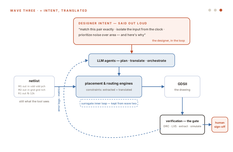
This is why the ninety seconds matters more than the headline. MAGICAL’s measured performance is what got the paper published; the synthesis time is what I’d build a company on. No single drawing was ever the expensive part of this job, and neither was any single simulation. The expensive part is entering a search with no known termination: the month that disappeared into the unbuildable amplifier, or the silicon-proven block nobody will touch even though a better path has a solid thesis behind it, because the known-good option has a bounded cost and the promising one doesn’t. The tool that matters isn’t the one that guesses your intent best on the first try. It’s the one that makes the tenth try cost what the first one did—because what that buys is the speed of finding out you’re wrong. The verification wall doesn’t vanish in this picture; finalists still pay full price at signoff. What collapses is everything before the finalists.
One consequence of all this, which I haven’t seen anyone state, so let me be the one the vendors get to argue with. Intent is easiest to write down on circuits you’ve built many times, because the wrong paths are already behind you—and those are exactly the circuits where a competent engineer is already fast, and where generators and IP reuse have been eating the work for a decade. Intent is weakest on leading-edge blocks with a new spec envelope, which is exactly where the schedule goes. So tools built to capture intent from a designer will perform best on the least valuable work, and the demos will look terrific. Migration is the honest exception—retargeting silicon-proven IP is high-value—but those tools aren’t capturing intent from a person. They’re mining it from an artifact in which every wager has already been settled.
Final thoughts
Let me make this falsifiable. My prediction is that within five years, the routine use of these tools won’t be “generate my layout”—it will be “regenerate it.” The win will show up as the number of physical iterations a block can absorb before tape-out, not the number of blocks generated from scratch. I’d count myself wrong if a production team ships a novel high-performance analog block whose layout was generated once, from a netlist, and accepted essentially as drawn. I’d count myself right if the first metric commercial analog automation competes on is turnaround time on a changed constraint, rather than area or match to a golden layout. And while I’m making claims: nobody in this field has published a benchmark I’d accept as a practitioner. The exam I want is boring—take a silicon-proven block, change one constraint late, and measure what it costs to get back to signoff.
My coworker’s smirk has aged well. Push-button analog layout for arbitrary circuits still hasn’t arrived, and I don’t expect it this decade. But the goal quietly moved—not from replacing the designer’s judgment to amplifying it, which is the framing vendors prefer, but from getting the intent right to finding out cheaply that it was wrong. The sculptor still has their hands on the clay. What changed is that the clay can finally hear them, and that you can ask it again tomorrow without starting over.
There’s one question I can’t shake. These systems learn from the accumulated intuition of veteran designers—intuition built through years of drawing polygons by hand, failing, and developing a feel for the clay. If the next generation never draws the polygons, where does the next generation’s physical intuition come from? Ask me again in thirty years.
Footnotes
Throughout, I mean custom analog and mixed-signal physical layout. Circuit sizing, topology selection, verification, and process migration are related stages, but a system that sizes an amplifier is not automatically a system that can place and route it, and conflating them is how this field’s history gets misread. I’m also deliberately vague about employers, products, and exact frequencies throughout, for the usual reasons.↩︎
Scheible and Lienig make a sharper version of this argument in “Automation of Analog IC Layout: Challenges and Solutions” (ISPD 2015): a digital flow gives up its degrees of freedom stepwise, in mostly separated sequential stages, while analog design gives them up continuously, with device generation, placement, and routing sometimes happening at once. That overlap is why you can’t just bolt a digital placer onto analog: analog layout is not primarily a packing problem, and treating devices as black boxes to pack optimally produced layouts that were compact and wrong.↩︎
For the sticklers: this assumes a voltage-feedback architecture—current-feedback amplifiers obey different rules. Scaling every resistor in the feedback network by the same factor leaves the ideal gain untouched; the side effects enter through thermal noise, bias-current error, loading, and parasitic capacitance. The point is not that one universal rule connects resistance to performance, but that physical choices participate in several interacting objectives at once.↩︎
I grade evidence in this field on four rungs, top to bottom: measured silicon, post-layout simulation, tool benchmark, demonstration. Almost everything published lives on the bottom two rungs, which is worth remembering when a result sounds like the problem is solved. MAGICAL’s ADC (CICC 2021) is one of the very few results on the top rung, which is why it anchors the post. Note what it did and didn’t establish: that a substantially automated flow can produce a real mixed-signal chip—not that any analog block at any node can be generated from a netlist. The flow still depended on foundry templates, extracted constraints, and optional design guidance.↩︎
The LayoutCopilot paper (IEEE TCAD 2025) also reports that one instructed multi-agent configuration reached 96.8% on 1,250 synthetic test cases—against the authors’ own sanity-check criteria, with the deeper manual functionality check covering only 25 of the passing cases. So “96.8%” should not be read as a universal layout-success rate, however much it sounds like the problem is nearly solved. If only! It remains the most practitioner-relevant academic tool I’ve seen, precisely because it’s built for interactive adjustment rather than one-shot generation.↩︎
With the usual caveats attached. GLayout’s 22-billion-parameter model completed 70% of its open evaluation tasks, and separately produced DRC- and LVS-clean results on unseen four-transistor blocks—meaningful, but far from production-scale synthesis. EEsizer’s funnel: eight models were tried on six basic circuits, three advanced to a 20-transistor rail-to-rail op amp, and only one of those (OpenAI’s o3) met the targets at the 90 nm predictive-technology node. And EEsizer is sizing, not layout—the architecture is what matters: the model proposes and interprets; the simulator decides whether the proposal worked.↩︎